Technologies
Many companies have already explored diffractive optical elements (DOEs) and deliberately chose not to use them. Often for understandable reasons: development was considered complex, manufacturing was expensive, and the practical benefits did not seem to justify the effort.
Today, however, that decision is worth revisiting. New manufacturing technologies and more powerful simulation methods have fundamentally changed what is possible with DOEs in recent years.
Choosing the right technology matters. But whether it becomes a competitive advantage depends on the expertise behind its development, simulation, and manufacturability.
Why DOEs May Be Worth Reconsidering Today
Diffractive optical elements do not replace conventional optics across the board. They extend their capabilities, enabling optical functions that would often require significantly greater effort with conventional optical systems—or, in some cases, could not be achieved at all.
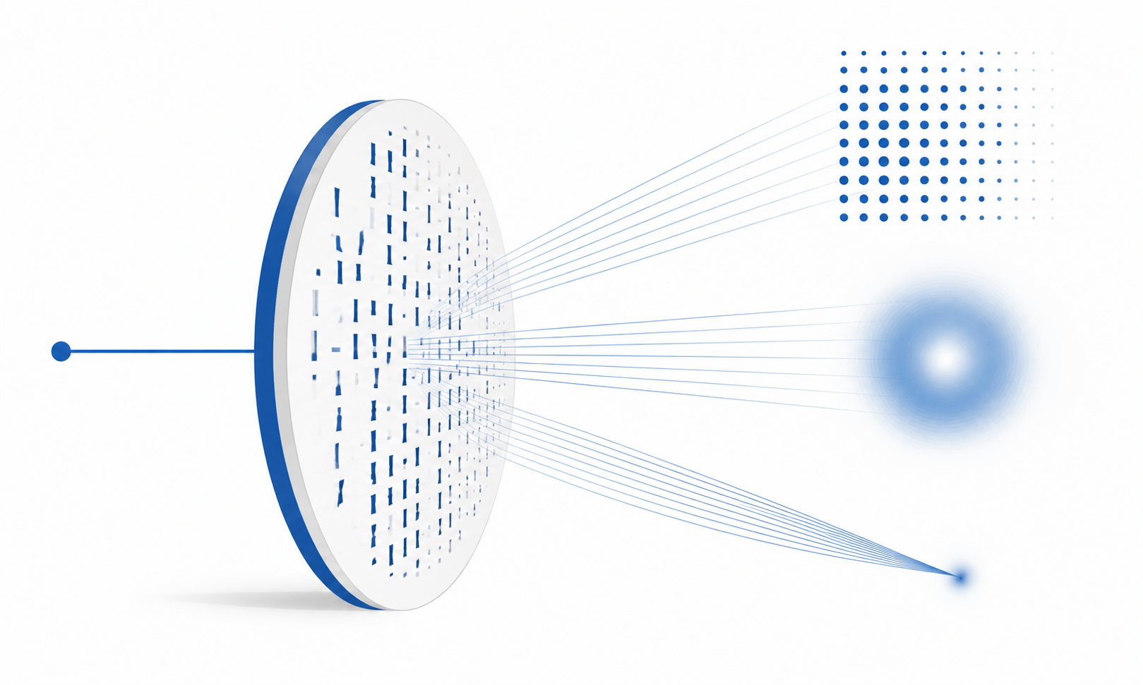
For companies, the payoff is real. Multiple optical functions can often be combined in a single component. This can make optical systems more compact, reduce the number of components, and simplify alignment. At the same time, DOEs enable functions such as structured illumination for 3D sensing, precise beam shaping for LiDAR systems, and uniform energy distribution in laser systems. This opens up new possibilities for applications in medical technology, sensing, metrology, and autonomous driving.
One example is the active intraocular lens that Helbling developed in collaboration with Elenza, a US medical-device company. In this system, a DOE combined with a liquid crystal cell enables the optical power to adjust automatically, thereby simulating the human eye’s natural ability to accommodate. As a result, patients can see objects clearly at different distances without having to rely on multiple optical systems.
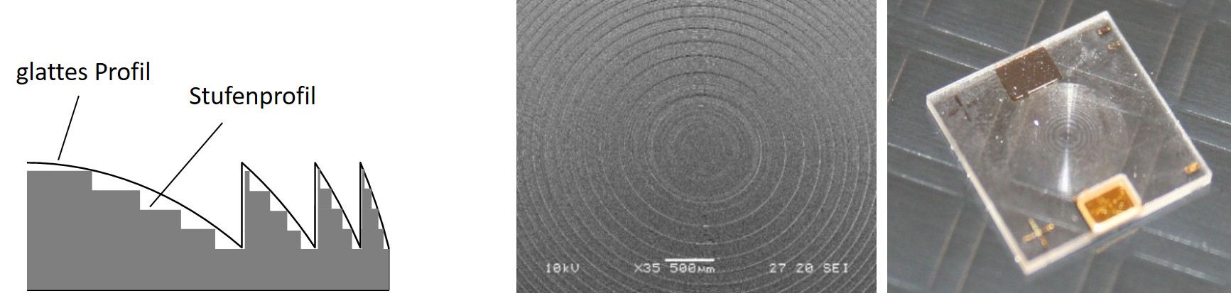
Just a few years ago, many of these applications were barely economically viable. Modern manufacturing processes such as nanoimprinting, wafer-level production, injection molding, and direct laser writing are changing the equation. They enable more precise and cost-effective production, making DOEs increasingly attractive for higher volumes as well.
The Real Challenge Is Rarely the Idea
Many DOE projects begin with a compelling technical idea. The difficulties often emerge only later.
One typical challenge is manufacturability. A DOE may deliver outstanding results in simulation yet fail when confronted with real-world manufacturing tolerances, or prove feasible only at disproportionate cost. The development effort is also frequently underestimated.
Another common pitfall is the choice of simulation model. If the model is based on unsuitable assumptions, simulated and actual performance can differ considerably. This leads to unnecessary iterations, additional prototypes, and rising development costs.
“A simulation model based on unsuitable assumptions produces incorrect results and leads to failure.”
Dr. Helen Wächter
Material selection, manufacturing technology, and achievable precision therefore should not be considered only toward the end of a project. They need to be addressed during the concept phase.
Successful Projects Make the Right Decisions Early
The difference between successful and unsuccessful DOE projects often lies not in the quality of the idea, but in the decisions made at the start of development.
Successful projects ask the critical questions early. What optical function is actually required? Which simulation model represents the underlying physics with sufficient accuracy? Which manufacturing technology is suitable for the intended application? What tolerances can realistically be achieved? And can the design later be manufactured economically at scale?
Different methods are available for modeling, including Rigorous Coupled-Wave Analysis (RCWA), the Thin Element Approximation (TEA), the Beam Propagation Method (BPM), and the Wave Propagation Method (WPM). Each has specific strengths and limitations. The key is not to choose the most powerful method, but the one whose assumptions fit the task at hand. This is often where a project either gains momentum or stalls, burning through time and budget on avoidable iterations.
Navigating Between Enthusiasm and Dismissal
Conversations with companies repeatedly reveal the same pattern: some regard DOEs as an almost universal solution to optical challenges. Others dismiss them outright because they consider them too complex or too expensive.
Neither approach is likely to produce the best results.
For companies that work with diffractive optical elements only occasionally, it is particularly difficult to assess which designs are comparatively straightforward to implement and which place high demands on simulation, manufacturing, or tolerances. A sound assessment therefore requires experience across the entire development process.
This is Just the Beginning
The field continues to evolve rapidly.
One particularly exciting development is the transition from conventional DOEs to metasurfaces and nanostructures. These enable ultrathin optical elements and functions that are difficult or impossible to realize with conventional optics, such as polarization-dependent optics. At the same time, modern manufacturing technologies are continuing to advance miniaturization and high-volume integration.
For companies, the real lesson is this: a technology decision that was right a few years ago may no longer be the right one today.
“Manufacturing methods for DOEs have advanced considerably in recent years. It is worth reassessing today whether a DOE could be a suitable solution for an optical system.”
Dr. Helen Wächter
Expertise Turns Potential into Market-Ready Innovation
Diffractive optical elements therefore open up new possibilities. To turn that potential into a lasting competitive advantage, companies need to pinpoint where DOEs add real value and which development strategy fits the application. Crucially, they must also identify risks while the project is still in the concept phase.
As a technology-independent development partner, Helbling supports companies from evaluating different solution approaches and selecting suitable simulation methods through to manufacturing-ready development.
The difference between a good idea and a successful innovation is rarely determined on the factory floor. It is decided at the very beginning of development.
Author: Dr. Helen Wächter Fischer
Main Image: Helbling